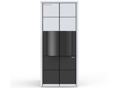
The Themis S S/TEM is an 80–200kV scanning / transmission electron microscope (S/TEM) designed for high-speed imaging and analysis of semiconductor devices. As the latest member of the industry-standard Themis family, the Themis S TEM inherits a unique combination of the best spatial resolution and the most efficient chemical analysis.
The Themis S S/TEM benefits for Semiconductors include:
Fastest time to data Themis S S/TEM achieves the fastest time to data by using a combination of the Piezo stage and drift corrected frame integration (DCFI) to compensate for possible specimen drift. This makes it possible to acquire high-quality high-resolution images in both TEM and STEM modes only minutes after sample loading. Optimized productivity To optimize productivity, Themis S S/TEM uses double-coil constant power lenses to minimize the thermal drift and maximize the system throughput. This design eliminates heating variation in the lens when switching between modes, such as changing from low-magnification mode for feature searching and high-magnification mode for imaging. 声明:本网部分文章和图片来源于网络,发布的文章仅用于材料专业知识和市场资讯的交流与分享,不用于任何商业目的。任何个人或组织若对文章版权或其内容的真实性、准确性存有疑义,请第一时间联系我们,我们将及时进行处理。 |
小黑屋|手机版|Archiver|版权声明|一起进步网
( 京ICP备14007691号-1 ) 
GMT+8, 2024-4-17 02:13 , Processed in 0.210073 second(s), 38 queries .
Powered by Discuz! X3.2
© 2001-2013 Comsenz Inc.